According to the Shell Sky Scenario, photovoltaics (PV) will need to reach a production capacity of 1000 GW per year from the year 2035 onwards to follow the Paris agreement and stay below 2 degrees of increase in global temperatures. This represents a phenomenal growth rate compared to today’s total installed capacity of about 600 GW (for reference, the capacity added last year was about 140 GW).
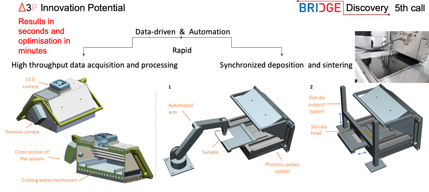
This project investigates the novel flash infrared annealing (FIRA) technique to produce thin-film materials based on perovskite-silicon tandem solar cells. This solar cell technology has the potential to accelerate the deployment of PV thanks to its potential for high performance and low fabrication costs. The specific objective of this project is to industrialise the process thanks to a multidisciplinary approach involving mechanical, electrical, electronics and and data science engineerings. The potential is enormous, targeting highly efficient perovskite-silicon tandem solar cells (~30% efficiency) at fraction (1/10) of the environmental impact involved with traditional Si cells.
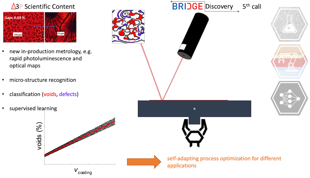
The specific contribution of iCoSys will be to analyse the data acquired from new in-production metrology, e.g. rapid photoluminescence and optical maps, structure recognition, classification (voids, defects) supervised learning. Thanks to an automation of the process, the quantity of data will allow such approaches.